Week 14: Build the MCU
Goal. Put every block together into a working 4-bit microcontroller, load a small program into its ROM, and step through it. This is the whole course in one circuit.
Open the MCU
The complete machine runs in LogicLab. Open it, press power, and single-step the clock to watch it execute:
▶ Open the 4-bit MCU in LogicLab
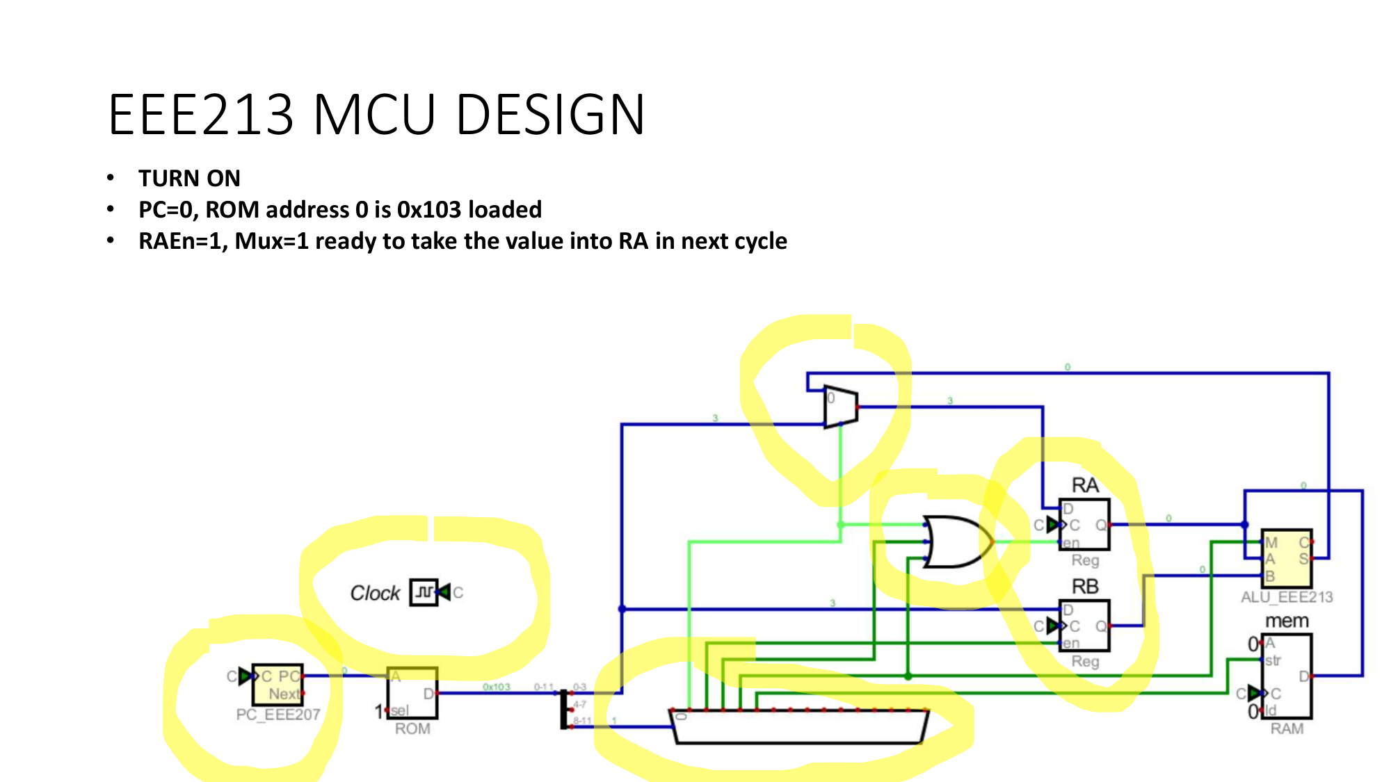
It is all blocks you have built
LogicLab now provides each datapath part as a single block, so the MCU is a small diagram rather than a sea of gates. Every block is something you built up from gates in an earlier week:
- CNT4 is the program counter (the counter from Week 11): it holds the address of the next instruction.
- ROM8 holds the program (the memory from Week 13); the PC addresses it and it returns the instruction word as a parallel output.
- DEC4 and a couple of OR gates are the control logic (the decoder from Week 8): they read the instruction and raise the right control lines.
- MUX2 blocks route the data (the multiplexer from Week 8): they choose whether a register loads an operand or the ALU result.
- REG4 are the working registers RA and RB (the register from Week 12).
- ALU4 is the arithmetic unit (the adder/subtractor from Week 7).
- RAM8 is the data memory (also Week 13); STS writes a result into it.
Add the clock, and it is a computer.
The ROM is the program
The program lives in ROM8 as a parallel instruction word, split off to the decoder path (control) and the register path (operand). This is the program stored in it:
| Addr | Instruction | enA | enB | Mode | MUX | str | Operand |
|---|---|---|---|---|---|---|---|
| 0 | LDA 3 | 1 | 0 | 0 | 1 | 0 | 3 |
| 1 | LDB 2 | 0 | 1 | 0 | 0 | 0 | 2 |
| 2 | ADD | 1 | 0 | 0 | 0 | 0 | - |
| 3 | SUB | 1 | 0 | 1 | 0 | 0 | - |
| 4 | STS | 0 | 0 | 0 | 0 | 1 | - |
| 5-7 | NOP | 0 | 0 | 0 | 0 | 0 | - |
von Neumann vs Harvard
In the von Neumann architecture instructions and data share one memory; in the Harvard architecture they are separate (here, ROM8 for the program, RAM8 for data), so the machine can fetch an instruction and access data at once. Our MCU is Harvard.
Running the program
Each clock: CNT4 addresses ROM8, the instruction word drives DEC4 and the control OR
gates, those control lines set the MUX2 routing, the REG4 load enables, and the ALU4
mode, and the data flows accordingly. Tracing LDA 3; LDB 2; ADD; SUB; STS:
- LDA 3: the MUX picks the operand, enA loads it. RA = 3.
- LDB 2: enB loads the operand. RB = 2.
- ADD: Mode = 0, the MUX picks the ALU output, enA loads it. RA = 3 + 2 = 5.
- SUB: Mode = 1, enA loads the ALU output. RA = 5 - 2 = 3.
- STS: str writes RA into RAM8. RAM = 3.
A processor is a logic circuit, and you built every piece of it.
The proof it is real
Write the same program on an Arduino and run it. The gate-level MCU and the real microcontroller carry out the same steps and reach the same result. The listing and wiring are in the Lab Annex.
What is inside each block
If you want to see how a block works from gates rather than as a single part, these were built up in the earlier weeks: the ALU from full adders, the register and program counter from flip-flops, and the ROM from a lookup table.
Check yourself
- Trace
LDA 3; LDB 2; SUB; STS. What ends up in RAM? - Which control bit does only STS use, and what does it do?
- Why can a Harvard machine fetch an instruction and read data in the same cycle?