Week 1 — Why Verilog, and Gate-Level Modeling
The historical idea (why this comes first)
Verilog was created (by Philip Moorby, 1984) to verify logic — to test circuits that engineers had already designed by hand. “Verilog = Verification of Logic.” So we start where history did: you are handed a circuit diagram (from a datasheet or your own sketch) and your first job is to describe it in Verilog. Designing circuits with Verilog (synthesis) comes much later (Week 10).
Objectives
- Explain what an HDL is and why it appeared.
- Open VeriSim; place code in
design.v/testbench.v; run a simulation. - Describe a given gate circuit with primitives (
and,or,not,nand,nor,xor,xnor). - Name the gates (
G0, G1, …) and the wires (W1, W2, …) on the schematic.
Conventions (used throughout the course)
module halfadder(
    output S, C,      // outputs first
    input  A, B
);
    xor G0 (S, A, B); // primitive: instance name, then (output, inputs...)
    and G1 (C, A, B);
endmodule
Every gate gets a unique instance name (you may reuse the same gate type many times).
Internal connections between gates are wires you name W1, W2, …. If a signal’s type is
not declared, it is a 1-bit wire. We use Verilog-2001/2005 port style (grouped
output …, input …), not the older 1995 style.
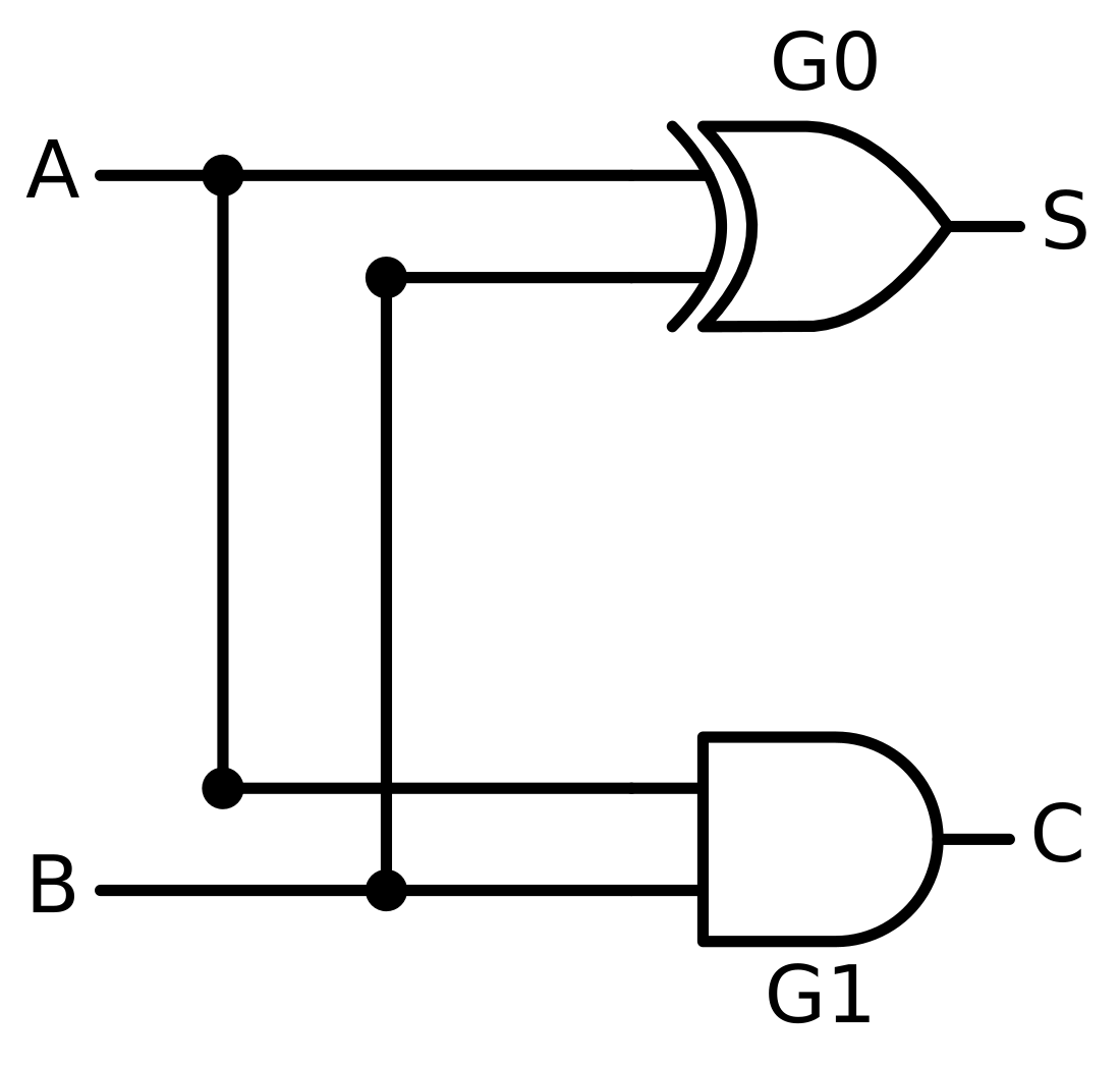
Example 1 — Half adder (a circuit you already know)
sum = A XOR B, carry = A AND B. Two gates, two lines.
design.v
// half adder
module halfadder(
    output S, C,
    input  A, B
);
    xor G0 (S, A, B);
    and G1 (C, A, B);
endmodule
Example 2 — Two AND gates: naming the wire between them
When two gates connect, the connecting node needs a name. That node is a wire.
design.v
// D = (A AND B) AND C
module twoand(
    output D,
    input  A, B, C
);
    wire W1;            // the node between the two AND gates
    and G0 (W1, A, B);  // W1 = A & B
    and G1 (D, W1, C);  // D  = W1 & C
endmodule
Example 3 — Full adder (more gates, more wires)
design.v
// full adder
module fulladder(
    output S, Co,
    input  A, B, Ci
);
    wire W1, W2, W3;
    xor G0 (W1, A, B);
    xor G1 (S,  W1, Ci);
    and G2 (W2, A, B);
    and G3 (W3, Ci, W1);
    or  G4 (Co, W2, W3);
endmodule
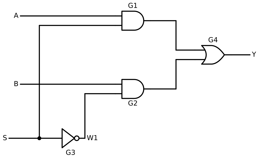
Example 4 — 2-to-1 MUX from gates
design.v
// MUX 2to1 : Y = S ? B : A   (built from primitives)
module mux2to1(
    output Y,
    input  A, B, S
);
    wire W1, W2, W3;
    not G3 (W1, S);       // W1 = ~S
    and G1 (W2, A, W1);   // W2 = A & ~S
    and G2 (W3, B, S);    // W3 = B & S
    or  G4 (Y, W2, W3);
endmodule
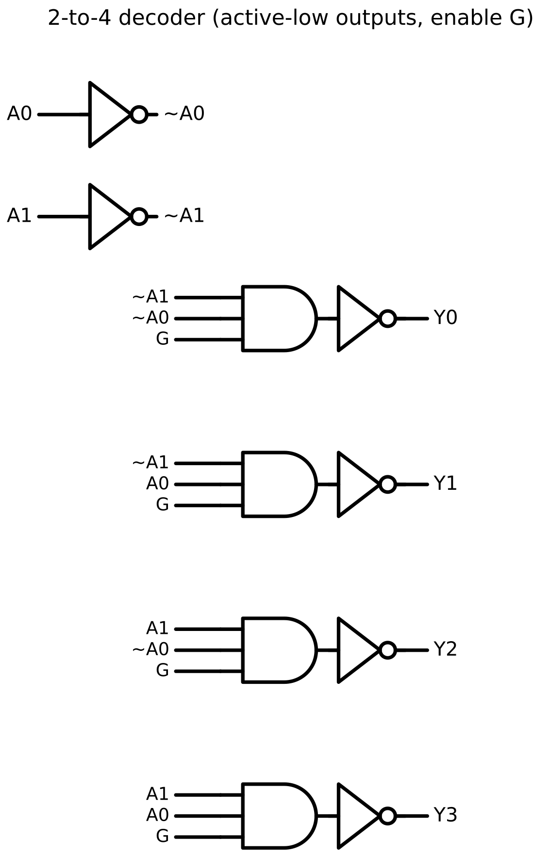
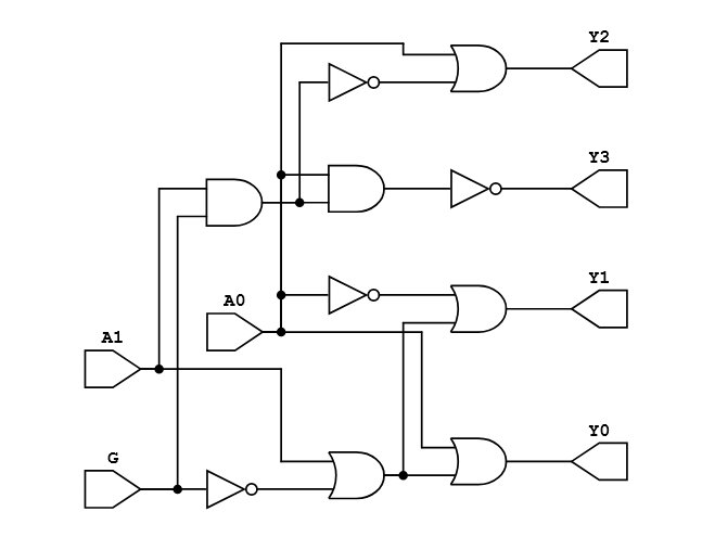
Example 5 — A datasheet circuit: gate-level 2-to-4 decoder
This is the practical one: a 74139-style active-low decoder with an enable G, transcribed
gate-by-gate from the logic diagram. Notice how every node on the drawing becomes a named wire.
design.v
// 2 to 4 line decoder (active-low outputs, active-high enable G)
module decoder(
    output Y0, Y1, Y2, Y3,
    input  A0, A1, G
);
    wire W1, W2, W3, W4, W5, W6, W7, W8, W9, W10;
    not G8  (W1, A0);          // W1 = ~A0
    not G9  (W2, A1);          // W2 = ~A1
    and G0  (W3, W2, W1);      // ~A1 & ~A0  -> 00
    and G1  (W4, W2, A0);      // ~A1 &  A0  -> 01
    and G2  (W5, A1, W1);      //  A1 & ~A0  -> 10
    and G3  (W6, A1, A0);      //  A1 &  A0  -> 11
    and G4  (W7,  W3, G);      // gate with enable
    and G5  (W8,  W4, G);
    and G6  (W9,  W5, G);
    and G7  (W10, W6, G);
    not G10 (Y0, W7);          // active-low outputs
    not G11 (Y1, W8);
    not G12 (Y2, W9);
    not G13 (Y3, W10);
endmodule
Behaviour (verified): with G=0 all outputs are 1 (disabled); with G=1 exactly the
selected output goes 0:
G A1 A0 : Y3 Y2 Y1 Y0
0  0  0 :  1  1  1  1   (disabled)
1  0  0 :  1  1  1  0
1  0  1 :  1  1  0  1
1  1  0 :  1  0  1  1
1  1  1 :  0  1  1  1
The IC logic diagram for this part lives in the manufacturer datasheet (TI SN74HCS139, “One of Two 2:4 Decoders”). Rather than copy that figure, the gate-level code above is your own redistributable transcription of it — and it is what students actually simulate.
Synthesizing this design (VeriSim’s Gates view) produces the same circuit automatically —
two inverters for A0/A1, AND gates gated by the enable G, and the active-low output stage:
Run any of these in VeriSim
- Open https://senolgulgonul.github.io/verisim/; paste a design into design.v.
- For now use the tiny testbench below (full testbench technique is Week 2):
`timescale 1ns/1ns
module tb;
    reg A, B;
    wire S, C;
    halfadder M0(.S(S), .C(C), .A(A), .B(B));   // named instantiation
    initial begin
        $dumpfile("dump.vcd"); $dumpvars(0, tb);
        $monitor("A=%b B=%b -> S=%b C=%b", A, B, S, C);
        A=0; B=0; #10; A=0; B=1; #10; A=1; B=0; #10; A=1; B=1; #10;
        $finish;
    end
endmodule
- Run, read the Console, open the Waveform (scroll=zoom, drag=pan, click=cursor).
What to look for
- Transcribing a diagram is mechanical once every node is named: one gate per line.
- The decoder’s outputs are active-low — the selected line goes to 0. This is the same active-low idea you will meet on the Tang Nano LEDs (Week 12).
Exercises (session 2)
- P, Q → Y. For the circuit handed out in class, name the wires on the drawing, write the
module with primitives, and a testbench that sweeps all four
PQinputs. - NAND-only AND. Build the AND function using only
nandgates (AND = NAND then NOT; NOT = one-input NAND). Name every wire. - 3-to-8 decoder. Extend the 2-to-4 decoder idea to 3 address bits (you may keep it gate-level or wait for behavioral modeling in Week 7 — try gate-level first).
- 1995 vs 2001 syntax. Rewrite the half adder in old (1995) port style and confirm it still simulates; note which style we use and why.