Week 5: Minimisation with Karnaugh maps
🏠 Home · Prev: Week 4 · Next: Week 6
Goal. Take the sum-of-products expression from the design chain and make it small, so the circuit uses fewer gates. We do this with Karnaugh maps, by eye, with three variables.
Why minimise
The minterm expression from Week 4 is always correct, but it is rarely the smallest. Fewer gates means a cheaper, faster, lower-power circuit. A Karnaugh map is a way to spot the simplifications visually instead of grinding through algebra.
Adjacency and the Gray-code order
A K-map is just the truth table folded into a grid so that neighbouring cells differ in one
variable. That is why the columns run 00, 01, 11, 10 and not 00, 01, 10, 11: each step
flips a single bit, so two adjacent 1s can always be combined.
The three-variable map
Plot a 1 in every cell whose minterm is 1, then circle the largest legal groups (sizes 1, 2, 4, 8: always a power of two), and read each group as the product of the variables that stay constant inside it.
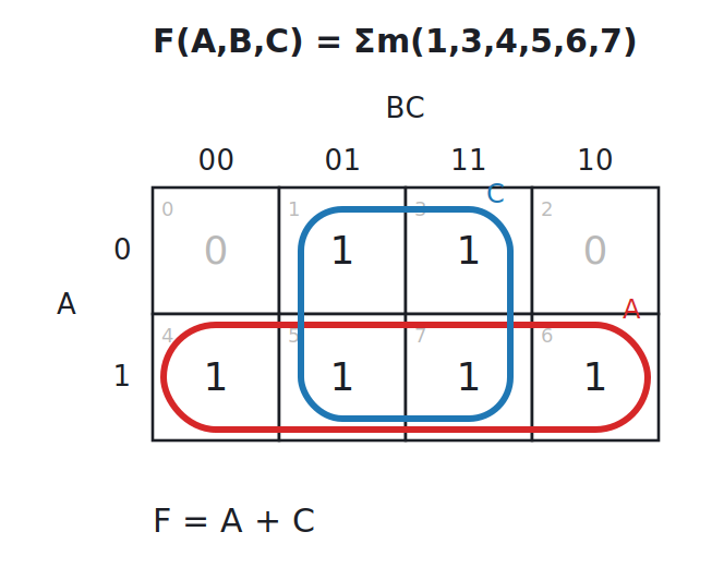
Here the bottom row is constant in A = 1, so it reads A; the middle two columns are constant
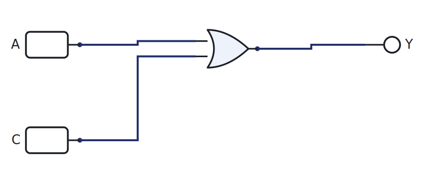
in C = 1, so they read C. The six-minterm expression collapses to F = A + C, a single OR
gate:
Grouping rules. Groups must be rectangles of 1, 2, 4, or 8 cells; bigger is better; every 1 must be covered at least once; groups may overlap; and the map wraps around, so the left and right edges (and top and bottom) are neighbours.
Don’t-care conditions
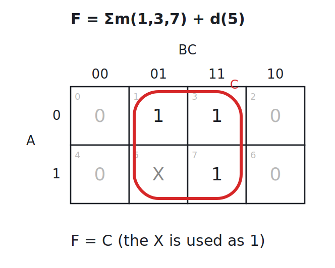
Sometimes an input combination can never happen, or its output does not matter. Mark it X, then
treat each X as a 1 or a 0, whichever makes a bigger group. Here the single X lets the C
column become a full group of four, so the answer is simply F = C:
Realising it with NAND or NOR only
By DeMorgan, any sum-of-products can be built from NAND gates alone, and any product-of-sums from NOR gates alone. Factories like this: one gate type, repeated. To convert an AND-OR circuit to NAND-NAND, replace every gate with a NAND and the logic is unchanged. Build both forms in LogicLab and toggle the inputs to confirm they agree.
XOR and parity
XOR is its own useful tool: it is 1 when its inputs differ. Chain XORs and you get a parity function, which is 1 when an odd number of inputs are 1. That is how a parity bit detects a single-bit error, and it reappears in the adder’s sum bit.
Reading a datasheet: active-high and active-low
On a real IC, a pin is active-high if it does its job when driven to 1, and active-low (marked with an overline) if it does its job when driven to 0. Reset and enable pins are very often active-low. Always check the datasheet’s logic table before you wire a part, because the silicon does not care which convention you assumed.
Try it yourself (optional)
Take a function, minimise it on paper, build the minimised circuit on the breadboard, and confirm with the Arduino that every input combination matches the original truth table. See the Lab Annex.
Check yourself
- Plot
F = Σm(0,2,4,6)on a 3-variable map and minimise it. (Hint: one group of four.) - Add the don’t-care
d(7)toF = Σm(3,5)and see whether it helps. - Convert
F = A·B + Cto a NAND-only circuit and verify it in LogicLab.