Week 14 — Microcontroller Architecture: Build a Tiny CPU
The historical idea
The course ends where digital design becomes programmable. A CPU is just a well-organized FSM (Week 11) wired to memory (Week 13) and an ALU (Week 6). We use AVR as the reference (students met it via Arduino), then build a minimal 4-bit MCU that runs a tiny program through fetch → decode → execute, see the same program run on a real AVR, and finish with a working single-cycle RISC-V (RV32I) core.
Objectives
- Explain von Neumann vs Harvard and what an instruction is.
- Describe fetch → decode → execute as a three-state FSM.
- Build a 4-bit accumulator MCU: ROM, ALU, registers, output.
- Run
LDA 3, LDB 2, ADD, ADD, SUB, STS→ 5 (3+2+2−2). - Run the same program on a real AVR, then on a single-cycle RISC-V (RV32I) core.
Concept (short)
- von Neumann: one memory for program + data. Harvard: separate memories (AVR is Harvard). The program counter (PC) holds the address of the next instruction.
- An instruction is a coded operation. Ours is 8 bits:
[7:4]opcode,[3:0]immediate. - The control unit is an FSM cycling FETCH (read instruction at PC) → DECODE (advance PC) → EXECUTE (do the operation).
| Opcode | Mnemonic | Action |
|---|---|---|
| 1 | LDA imm |
ACC ← imm |
| 2 | LDB imm |
B ← imm |
| 3 | ADD |
ACC ← ACC + B |
| 4 | SUB |
ACC ← ACC − B |
| 5 | STS |
OUT ← ACC |
| F | HLT |
stop |
Example 1 — building blocks you already have
Before the full CPU, note each piece is a circuit from earlier weeks:
// ALU (Week 6 dataflow): ADD/SUB on 4-bit operands
module alu4(input [3:0] a, b, input op, output [3:0] r);
    assign r = op ? (a - b) : (a + b);   // op=0 add, op=1 sub
endmodule

// a register (Week 8): loads on a clock edge
module reg4(input clk, input load, input [3:0] d, output reg [3:0] q);
    always @(posedge clk) if (load) q <= d;
endmodule
Example 2 — the whole 4-bit MCU
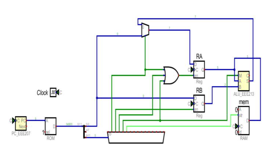
Verified in Icarus: produces OUT = 5, then halts. Here is the same machine drawn as a schematic,
built in Digital (Helmut Neemann): the ROM and program counter feed the instruction bus, the
two registers hold ACC and B, the ALU does add/sub, and the result is latched to the output
and RAM — every block one you built in earlier weeks.
design.v
module mcu4(input clk, input rst, output reg [3:0] out, output reg halted);
    localparam LDA=4'h1, LDB=4'h2, ADD=4'h3, SUB=4'h4, STS=4'h5, HLT=4'hF;
    localparam FETCH=2'd0, DECODE=2'd1, EXEC=2'd2;

    reg [7:0] rom [0:7];      // program memory
    reg [2:0] pc;             // program counter
    reg [7:0] ir;             // instruction register
    reg [3:0] acc, b;         // accumulator + B register
    reg [1:0] state;

    initial begin             // program bytes in HEX — these are exactly the values you see
        rom[0] = 8'h13;       // LDA 3 : ACC = 3        (opcode 1, immediate 3)
        rom[1] = 8'h22;       // LDB 2 : B   = 2        (opcode 2, immediate 2)
        rom[2] = 8'h30;       // ADD   : ACC = 3 + 2 = 5
        rom[3] = 8'h30;       // ADD   : ACC = 5 + 2 = 7
        rom[4] = 8'h40;       // SUB   : ACC = 7 - 2 = 5
        rom[5] = 8'h50;       // STS   : OUT = 5
        rom[6] = 8'hF0;       // HLT
        rom[7] = 8'hF0;       // HLT
    end

    always @(posedge clk or posedge rst) begin
        if (rst) begin
            pc<=0; acc<=0; b<=0; out<=0; halted<=0; ir<=0; state<=FETCH;
        end else case (state)
            FETCH:  begin ir <= rom[pc]; state <= DECODE; end
            DECODE: begin pc <= pc + 1'b1; state <= EXEC; end
            EXEC: begin
                case (ir[7:4])
                    LDA: acc <= ir[3:0];
                    LDB: b   <= ir[3:0];
                    ADD: acc <= acc + b;
                    SUB: acc <= acc - b;
                    STS: out <= acc;
                    HLT: halted <= 1'b1;
                endcase
                state <= (ir[7:4]==HLT) ? EXEC : FETCH;
            end
        endcase
    end
endmodule
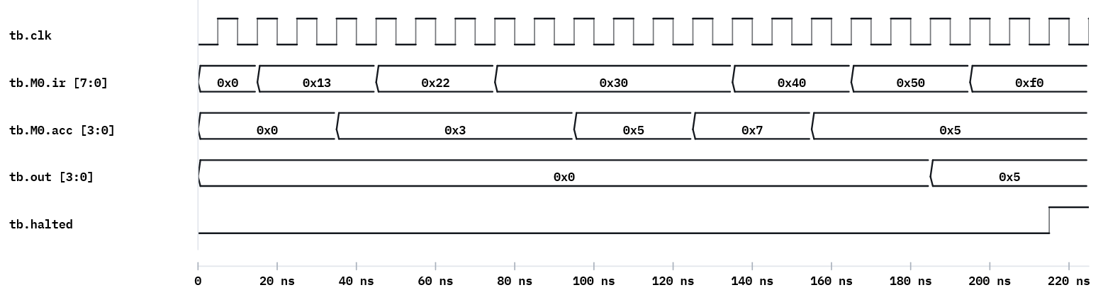
Each byte is opcode (high nibble) + immediate (low nibble), so 0x13 decodes as opcode 1
(LDA) with immediate 3, and 0xF0 is opcode F (HLT). These are exactly the hex values
that step across ir in the waveform below — handy for tracing the program by eye.
testbench.v
`timescale 1ns/1ps
module tb;
    reg clk = 0, rst = 1; wire [3:0] out; wire halted;
    mcu4 M0(.clk(clk), .rst(rst), .out(out), .halted(halted));
    always #5 clk = ~clk;
    initial begin
        $dumpfile("dump.vcd"); $dumpvars(0, tb);
        @(negedge clk) rst = 0;
        wait (halted == 1);
        @(posedge clk);
        $display("Program finished. OUT = %0d (expected 5), halted = %b", out, halted);
        if (out == 4'd5) $display("MCU TEST PASSED"); else $display("MCU TEST FAILED");
        $finish;
    end
endmodule
Expected Console
Program finished. OUT = 5 (expected 5), halted = 1
MCU TEST PASSED
Example 3 — on the board
Drive mcu4 from a divided clock, route out[3:0] to four LEDs (active-low), add a button
reset. After the program runs the LEDs show 0101 (= 5).
module mcu_board(input clk, input rst_btn, output [5:0] leds);
    localparam TICK = 5_000_000;
    reg [31:0] div = 0; reg slow = 0;
    always @(posedge clk) if (div==TICK) begin div<=0; slow<=~slow; end else div<=div+1;
    wire [3:0] out; wire halted;
    mcu4 cpu(.clk(slow), .rst(~rst_btn), .out(out), .halted(halted));
    assign leds = ~{2'b00, out};   // active-low
endmodule
Run it in VeriSim
- Run example 2 → MCU TEST PASSED (OUT = 5).
- On the Waveform, add
pc,state,acc,b,out. Watch the three-state cycle andaccmove 3 → 5 → 7 → 5. - Synthesize → RTL: identify the ROM, the PC register, the ALU adder, and the state register — the CPU as the blocks you already know.
The same program on a real AVR
The toy MCU is not a cartoon. The AVR chip on an Arduino Uno or Nano runs the same kind of
program — fetch → decode → execute over its own ISA — and you can write that assembly by hand
from inside an ordinary sketch, then read the answer back over the serial monitor.
Here is our 4-bit MCU program — LDA 3, LDB 2, ADD, ADD, SUB, STS → 5 (3 + 2 + 2 − 2) —
rewritten as AVR inline assembly. The mnemonics line up almost one-to-one with our toy
opcodes (LDA/LDB → ldi, ADD → add, SUB → sub, STS → sts):
// Arduino sketch — the 4-bit MCU program on a real AVR (Uno / Nano)
// Senol Gulgonul
volatile byte a = 0;

void setup() {
  Serial.begin(9600);
  asm volatile (
    "ldi r26, 3      \n"   // LDA 3 : ACC = 3
    "ldi r27, 2      \n"   // LDB 2 : B   = 2
    "add r26, r27    \n"   // ADD   : ACC = 3 + 2 = 5
    "add r26, r27    \n"   // ADD   : ACC = 5 + 2 = 7
    "sub r26, r27    \n"   // SUB   : ACC = 7 - 2 = 5
    "sts a, r26      \n"   // STS   : a = ACC = 5
    : : : "r26", "r27"      // tell the compiler these registers were used
  );
  Serial.print("a = ");
  Serial.println(a);        // Serial Monitor prints:  a = 5
}

void loop() { }
Flash it, open the Serial Monitor at 9600 baud, and you see a = 5 — the exact result your
4-bit mcu4 produced in VeriSim. Same idea, real silicon.
RISC-V
Our 4-bit MCU shows the principle. RISC-V is that same principle at industrial scale: an open-standard instruction set architecture (ISA) that anyone may implement free of license fees — which is why it now appears in microcontrollers, phones, and datacenter chips. The specifications are published openly at riscv.org, with the full ISA manuals under riscv.org/technical/specifications.
The base 32-bit integer ISA, RV32I, keeps the same fetch → decode → execute loop you just
built, but with 32-bit instructions, 32 general-purpose registers (x0–x31, where x0 is
hardwired to 0), and a wider decoder that recognises arithmetic, branch, jump, and load/store
formats. The diagram below is a single-cycle RV32I datapath — one instruction per clock —
which is exactly what the design.v further down implements:
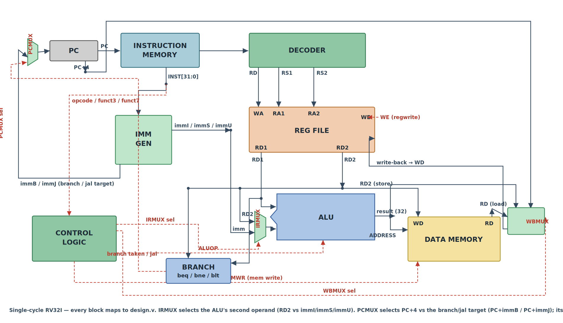
Just like the rom[] in our 4-bit MCU, we embed the program directly as machine code — so this
real (subset) RV32I core runs in VeriSim with no toolchain. It computes
sum = 1 + 2 + … + 10 = 55 with a genuine loop (addi, add, beq, jal) and stores the
result to data memory.
design.v
// Single-cycle RV32I (subset). The program is embedded inline (no $readmemh,
// no firmware), so it runs in VeriSim with no toolchain. Pair with testbench.v.

// register file: 32 x 32-bit, x0 hardwired to 0
module regfile(
    input             clk,
    input      [4:0]  rs1, rs2, rd,
    input             we,
    input      [31:0] wd,
    output     [31:0] rd1, rd2
);
    reg [31:0] r [0:31];
    integer k;
    initial for (k = 0; k < 32; k = k + 1) r[k] = 32'b0;
    assign rd1 = (rs1 == 5'd0) ? 32'b0 : r[rs1];
    assign rd2 = (rs2 == 5'd0) ? 32'b0 : r[rs2];
    always @(posedge clk)
        if (we && rd != 5'd0) r[rd] <= wd;
endmodule

// CPU core
module cpu(
    input             clk,
    input             rst,
    output reg [31:0] pc,
    output     [31:0] dmem0       // expose data memory word 0 for checking
);
    // instruction memory (word addressed)
    reg [31:0] imem [0:63];
    integer i;
    initial begin
        for (i = 0; i < 64; i = i + 1) imem[i] = 32'h00000013; // NOP
        imem[0] = 32'h00000093;   // addi x1, x0, 0     ; sum = 0
        imem[1] = 32'h00100113;   // addi x2, x0, 1     ; i = 1
        imem[2] = 32'h00b00193;   // addi x3, x0, 11    ; limit = 11
        imem[3] = 32'h00310863;   // beq  x2, x3, done
        imem[4] = 32'h002080b3;   // add  x1, x1, x2    ; sum += i
        imem[5] = 32'h00110113;   // addi x2, x2, 1     ; i++
        imem[6] = 32'hff5ff06f;   // jal  x0, loop
        imem[7] = 32'h00102023;   // sw   x1, 0(x0)     ; done: store sum
        imem[8] = 32'h0000006f;   // jal  x0, 0         ; halt (self loop)
    end

    // data memory
    reg [31:0] dmem [0:63];
    initial for (i = 0; i < 64; i = i + 1) dmem[i] = 32'b0;
    assign dmem0 = dmem[0];

    // fetch
    wire [31:0] instr = imem[pc[31:2]];

    // decode fields
    wire [6:0] opcode = instr[6:0];
    wire [4:0] rd     = instr[11:7];
    wire [2:0] f3     = instr[14:12];
    wire [4:0] rs1    = instr[19:15];
    wire [4:0] rs2    = instr[24:20];
    wire [6:0] f7     = instr[31:25];

    // immediates
    wire [31:0] immI = {{20{instr[31]}}, instr[31:20]};
    wire [31:0] immS = {{20{instr[31]}}, instr[31:25], instr[11:7]};
    wire [31:0] immB = {{19{instr[31]}}, instr[31], instr[7],
                        instr[30:25], instr[11:8], 1'b0};
    wire [31:0] immU = {instr[31:12], 12'b0};
    wire [31:0] immJ = {{11{instr[31]}}, instr[31], instr[19:12],
                        instr[20], instr[30:21], 1'b0};

    // register file
    wire [31:0] rdata1, rdata2;
    reg         regwrite;
    reg  [31:0] wdata;
    regfile RF(.clk(clk), .rs1(rs1), .rs2(rs2), .rd(rd),
               .we(regwrite), .wd(wdata), .rd1(rdata1), .rd2(rdata2));

    // ALU
    reg  [31:0] alu;
    always @(*) begin
        case (opcode)
            7'b0010011: begin                  // I-type ALU
                case (f3)
                    3'b000: alu = rdata1 + immI;                       // addi
                    3'b111: alu = rdata1 & immI;                       // andi
                    3'b110: alu = rdata1 | immI;                       // ori
                    3'b100: alu = rdata1 ^ immI;                       // xori
                    3'b001: alu = rdata1 << immI[4:0];                 // slli
                    3'b101: alu = rdata1 >> immI[4:0];                 // srli
                    3'b010: alu = ($signed(rdata1) < $signed(immI)) ? 32'd1 : 32'd0; // slti
                    3'b011: alu = (rdata1 < immI) ? 32'd1 : 32'd0;     // sltiu
                    default: alu = 32'b0;
                endcase
            end
            7'b0110011: begin                  // R-type
                case (f3)
                    3'b000: alu = (f7[5]) ? (rdata1 - rdata2) : (rdata1 + rdata2); // sub/add
                    3'b111: alu = rdata1 & rdata2;                     // and
                    3'b110: alu = rdata1 | rdata2;                     // or
                    3'b100: alu = rdata1 ^ rdata2;                     // xor
                    3'b001: alu = rdata1 << rdata2[4:0];               // sll
                    3'b101: alu = rdata1 >> rdata2[4:0];               // srl
                    3'b010: alu = ($signed(rdata1) < $signed(rdata2)) ? 32'd1 : 32'd0; // slt
                    3'b011: alu = (rdata1 < rdata2) ? 32'd1 : 32'd0;   // sltu
                    default: alu = 32'b0;
                endcase
            end
            7'b0110111: alu = immU;             // lui
            7'b0000011: alu = rdata1 + immI;    // lw  (address)
            7'b0100011: alu = rdata1 + immS;    // sw  (address)
            default:    alu = 32'b0;
        endcase
    end

    // branch decision
    reg branch_taken;
    always @(*) begin
        branch_taken = 1'b0;
        if (opcode == 7'b1100011)
            case (f3)
                3'b000: branch_taken = (rdata1 == rdata2);                  // beq
                3'b001: branch_taken = (rdata1 != rdata2);                  // bne
                3'b100: branch_taken = ($signed(rdata1) < $signed(rdata2)); // blt
                default: branch_taken = 1'b0;
            endcase
    end

    // write-back source select
    always @(*) begin
        regwrite = 1'b0;
        wdata    = 32'b0;
        case (opcode)
            7'b0010011, 7'b0110011, 7'b0110111: begin regwrite = 1'b1; wdata = alu;            end // ALU / lui
            7'b0000011:                         begin regwrite = 1'b1; wdata = dmem[alu[31:2]]; end // lw
            7'b1101111:                         begin regwrite = 1'b1; wdata = pc + 32'd4;      end // jal
            default: ;
        endcase
    end

    // next PC + sequential state
    always @(posedge clk) begin
        if (rst) pc <= 32'b0;
        else begin
            if (opcode == 7'b0100011) dmem[alu[31:2]] <= rdata2;   // sw
            if      (opcode == 7'b1101111) pc <= pc + immJ;        // jal
            else if (branch_taken)         pc <= pc + immB;        // taken branch
            else                           pc <= pc + 32'd4;
        end
    end
endmodule
testbench.v
`timescale 1ns/1ps
module tb;
    reg clk = 0, rst = 1;
    wire [31:0] pc, dmem0;
    cpu M0(.clk(clk), .rst(rst), .pc(pc), .dmem0(dmem0));
    always #5 clk = ~clk;
    integer cyc;
    initial begin
        $dumpfile("dump.vcd"); $dumpvars(0, tb);
        rst = 1; #12 rst = 0;                       // hold reset across first edge
        for (cyc=0; cyc<60; cyc=cyc+1) @(posedge clk);  // run the program
        $display("Program finished. dmem[0] = %0d (expected 55)", dmem0);
        if (dmem0 === 32'd55) $display("RISC-V TEST PASSED");
        else                  $display("RISC-V TEST FAILED");
        $finish;
    end
endmodule
Expected Console
Program finished. dmem[0] = 55 (expected 55)
RISC-V TEST PASSED
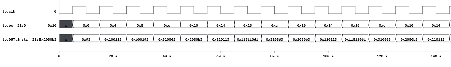
The waveform shows the loop body running: pc walks 0xc → 0x10 → 0x14 → 0x18 and jumps back to
0xc ten times while instr cycles through the encoded words, leaving 55 in data memory at
the end.
This is where the course points next. The same three steps you have used all term — describe,
simulate, synthesize — scale directly from a 4-bit toy to a production ISA. RV32I makes a
natural capstone: extend the core with more lw/sw exercises, add instructions from the
RISC-V specifications, or target the Tang Nano 9K.
(Subset implemented: LUI, ADDI, ADD, SUB, AND, OR, XOR, SLL, SRL, SLT, SLTU, BEQ, BNE, BLT, JAL,
LW, SW. Single-cycle for clarity; pipelining and CSR/privilege come later.)
Exercises (session 2)
- Extend the ISA. Add
AND,OR, andJMP imm(set PC). Write a looping program with aHLT. - Wider data. Promote the datapath to 8 bits; run a program that would overflow 4 bits to show why width matters.
- Project seed. Implement a small program (e.g. a running sum on LEDs) end-to-end: simulate in VeriSim, then run on the Tang Nano 9K.
Course wrap-up
In fourteen weeks students followed Verilog’s own history: describe a circuit and test it, then learn to synthesize it, then implement it on an FPGA — ending with a small CPU running a program on real silicon. Every step was verified in VeriSim first.