Week 12 — FPGA & the Tang Nano 9K: The Third Use of Verilog
The historical idea — three uses of Verilog
- Describe & simulate a hand-designed circuit (Weeks 1–9, 11).
- Synthesize — let the tool build the circuit (Week 10).
- FPGA implementation — load that circuit onto reconfigurable silicon (now).
An FPGA is field-programmable: instead of fixed gates it has Configurable Logic Blocks of Look-Up Tables. A 4-input LUT is a 16×1 memory — program its cells and it computes any 4-input function. Your synthesized netlist becomes a LUT/flip-flop configuration (the bitstream).
Objectives
- Explain CLB / LUT.
- Identify the Tang Nano 9K peripherals: LEDs, buttons, clock.
- Set up a Gowin project for GW1NR-9C (
GW1NR-UV9QN88PC6/I5) and write a.cstfile. - Run the flow: synthesize → floor planner → place & route → programmer → schematic viewer.
The board (one per student)
| Resource | Pin(s) | Polarity |
|---|---|---|
| Clock (27 MHz) | 52 | — |
| LEDs (6) | 10, 11, 13, 14, 15, 16 | active-LOW (lit when pin = 0) |
| Button S1 | 4 | active-LOW (pressed = 0) |
| Button S2 | 3 | active-LOW (pressed = 0) |
LEDs are common-anode from the supply, so drive a pin low to light it. Keep logic positive and invert once at the pins. Gowin EDA is free, no license.
The board itself (one per student). Front — USB-C, the two buttons S1 and S2, and the GW1NR FPGA (marked “TANG NANO 9K / SiPEED”):
Back — the pin-number silkscreen down both header rows. These are exactly the numbers you
put in the .cst constraints file (e.g. LEDs 10/11/13/14/15/16, clock 52):
A board running a design, with the on-board LEDs lit:
The Gowin IDE flow (slides 197–206)
The full flow on a tiny buffer (assign out = in;) project, end to end.
1. New Project → FPGA Design Project, then name it in the Project Wizard.
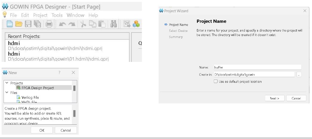
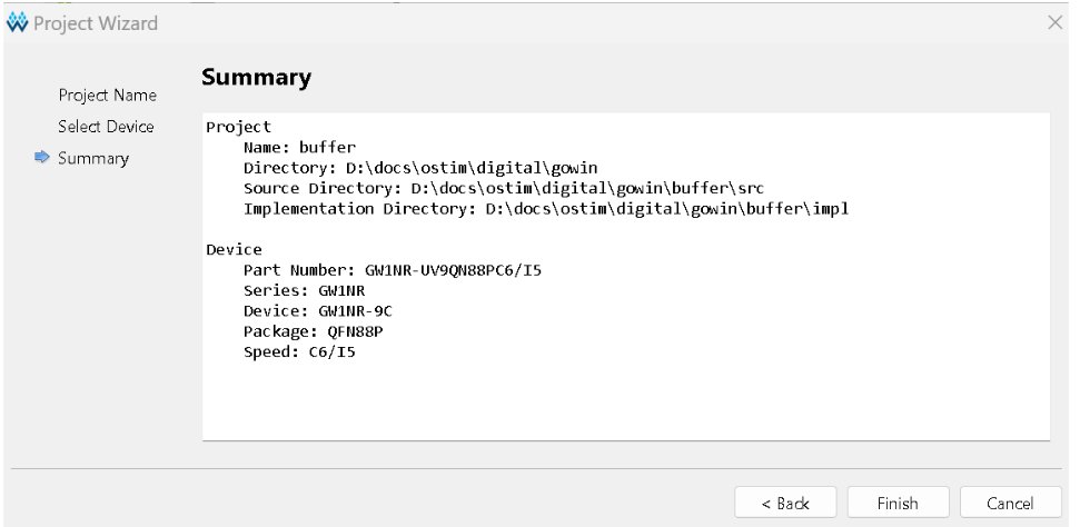
2. Select Device → Summary. This board is series GW1NR, part
GW1NR-UV9QN88PC6/I5, device GW1NR-9C, package QFN88P, speed C6/I5. Confirm on
the Summary page (match it to your board’s silkscreen).
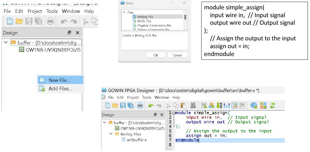
3. Add a Verilog file (here buffer.v with the simple_assign module). A .cst
constraints file is added later (step 6).
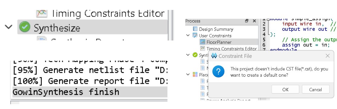
4. Process panel → Synthesize. Right-click Synthesize → Run. Configuration exposes options such as Dual-Purpose Pins (e.g. “Use DONE as regular IO”).
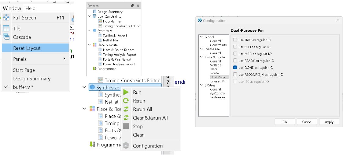
5. Synthesis finishes (green check; console shows GowinSynthesis finish). If there is no
.cst yet, Gowin offers to create a default one.
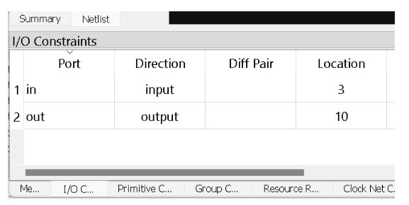
6. Floor Planner → I/O Constraints. Assign ports to physical pins. For buffer, in →
pin 3 (button S2) and out → pin 10 (LED0). This writes the .cst.
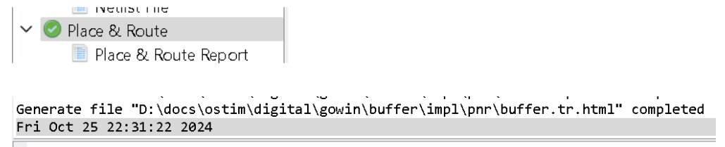
7. Place & Route → generates the bitstream (a .tr.html timing report is produced).
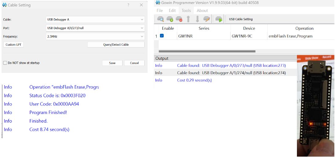
8. Programmer → pick the USB Debugger cable; write to SRAM (fast, volatile) or Flash
(persistent). The log ends with Program Finished! and the board lights up.
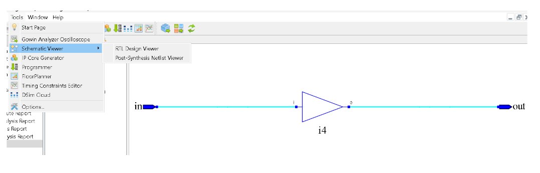
9. Schematic Viewer (Tools → Schematic Viewer → RTL Design Viewer / Post-Synthesis
Netlist Viewer) — the on-board analogue of VeriSim’s RTL view. For buffer it is a single
buffer from in to out.
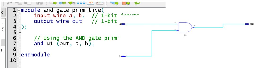
The Schematic Viewer also shows gate-level designs. Here an and_gate_primitive
(and u1 (out, a, b);) appears as a single AND gate u1 — the same primitive you wrote in
Week 1, now realized on the device:
Example 1 — AND gate to an LED (his example)
Two buttons in, one LED out — derived through the active-low hardware.
design.v
module and_demo(input s1, input s2, output led);
    // buttons pressed = 0; LED lit = 0.
    // "light when BOTH pressed": both pressed = (~s1 & ~s2); lit means output 0 -> invert.
    assign led = ~(~s1 & ~s2);     // simplifies to (s1 | s2)
endmodule
testbench.v
`timescale 1ns/1ns
module tb;
  reg s1, s2;
  wire led;
  and_demo dut(.s1(s1), .s2(s2), .led(led));
  initial begin
    $dumpfile("dump.vcd"); $dumpvars(0, tb);
    $display("s1 s2 | led (0 = lit)");
    s1=1; s2=1; #1 $display(" %b  %b |  %b", s1, s2, led);
    s1=1; s2=0; #1 $display(" %b  %b |  %b", s1, s2, led);
    s1=0; s2=1; #1 $display(" %b  %b |  %b", s1, s2, led);
    s1=0; s2=0; #1 $display(" %b  %b |  %b", s1, s2, led);
    $finish;
  end
endmodule
Expected (Icarus): led=0 only when both buttons are pressed (s1=s2=0).
and_demo.cst
IO_LOC  "s1"  4;  IO_PORT "s1"  PULL_MODE=UP;
IO_LOC  "s2"  3;  IO_PORT "s2"  PULL_MODE=UP;
IO_LOC  "led" 10; IO_PORT "led" PULL_MODE=UP DRIVE=8;
Example 2 — Half adder on the board
Reuse your verified halfadder: two buttons → two LEDs (sum and carry).
design.v
module half_adder_board(input s1, input s2, output [1:0] led);
    wire a = ~s1, b = ~s2;          // active-low buttons -> positive logic
    wire sum   = a ^ b;
    wire carry = a & b;
    assign led = ~{carry, sum};     // active-low LEDs
endmodule
testbench.v
`timescale 1ns/1ns
module tb;
  reg s1, s2;
  wire [1:0] led;
  half_adder_board dut(.s1(s1), .s2(s2), .led(led));
  initial begin
    $dumpfile("dump.vcd"); $dumpvars(0, tb);
    $display("s1 s2 | led = ~(carry,sum)");
    s1=1; s2=1; #1 $display(" %b  %b |  %b", s1, s2, led);
    s1=1; s2=0; #1 $display(" %b  %b |  %b", s1, s2, led);
    s1=0; s2=1; #1 $display(" %b  %b |  %b", s1, s2, led);
    s1=0; s2=0; #1 $display(" %b  %b |  %b", s1, s2, led);
    $finish;
  end
endmodule
Expected (Icarus): 11, 10, 10, 01 — both pressed gives carry (led=01).
half_adder_board.cst
IO_LOC  "s1"     4;  IO_PORT "s1" PULL_MODE=UP;
IO_LOC  "s2"     3;  IO_PORT "s2" PULL_MODE=UP;
IO_LOC  "led[0]" 10; IO_PORT "led[0]" PULL_MODE=UP DRIVE=8;
IO_LOC  "led[1]" 11; IO_PORT "led[1]" PULL_MODE=UP DRIVE=8;
Example 3 — if-else pattern selector
Press a button to switch between two LED patterns.
design.v
module ifelse_demo(input s1, output [5:0] leds);
    reg [5:0] pattern;
    always @(*) begin
        if (s1 == 1'b0) pattern = 6'b101010;   // S1 pressed
        else            pattern = 6'b010101;
    end
    assign leds = ~pattern;                     // invert once, at the pin boundary
endmodule
testbench.v
`timescale 1ns/1ns
module tb;
  reg s1;
  wire [5:0] leds;
  ifelse_demo dut(.s1(s1), .leds(leds));
  initial begin
    $dumpfile("dump.vcd"); $dumpvars(0, tb);
    s1=1; #1 $display("s1=%b leds=%b", s1, leds);
    s1=0; #1 $display("s1=%b leds=%b", s1, leds);
    $finish;
  end
endmodule
Expected (Icarus): s1=1 -> 101010, s1=0 -> 010101 (depends on s1 only).
(Constraints: s1 on 4; leds[0..5] on 10/11/13/14/15/16 — see the reference file.)
Verify in VeriSim, then build
- In VeriSim, test each design over the relevant button combinations (reading LEDs as
inverted:
led=0means lit). - In Gowin: New Project → GW1NR-9C → add
design.v+.cst→ Synthesize → Place & Route → Program (SRAM to test). - Press buttons; confirm the LED behaviour matches simulation after inversion.
What to look for
- Same source, two destinations. The design file is identical between VeriSim and Gowin.
- Active-low is not a bug. Derive
~(~s1 & ~s2)rather than memorizing it. - Compare Gowin’s Schematic Viewer with VeriSim’s RTL view of the same module.
Exercises (session 2)
- OR / XOR on the LED. Re-derive the constraint-correct expression for “lit when either pressed” and “exclusive-or”; program and confirm.
- Three LEDs at once. Show
s1,s2, ands1 ^ s2on LEDs 10/11/13. - Decoder on board. Put the Week-7 behavioral 2-to-4 decoder on four LEDs, driven by the two buttons.
- SRAM vs Flash. Program to SRAM, power-cycle (gone); to Flash, power-cycle (persists). Explain in one sentence.