Week 8 — Sequential Design: D Flip-Flop, Timescale & Waveforms
The historical idea
Until now outputs depended only on current inputs (combinational). Sequential circuits
remember: they update on a clock edge. With clocks in play, time becomes central — so
`timescale and the waveform stop being optional and become how you read a design.
Objectives
- Describe an edge-triggered D flip-flop with
always @(posedge Clk). - Build a 1-bit register with enable and a multi-bit register.
- Build a shift register.
- Read
`timescale unit/precisionand generate a clock in a testbench.
Concept (short)
A flip-flop captures D on the rising edge:
always @(posedge Clk) Q <= D; // non-blocking <= for clocked logic (full story Week 9)
`timescale 1ns/1ps = unit 1 ns (what #1 means), precision 1 ps (the rounding
grid). The midterm’s 1ns/100ps rounds delays to 100 ps. Generate a clock in the testbench:
reg clk = 0;
always #1 clk = ~clk;   // 2 ns period
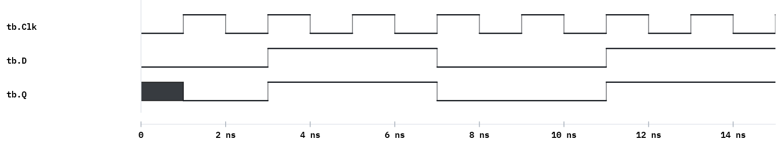
Example 1 — D flip-flop (his form)
design.v
// D flip-flop without reset
module DFF(
    output reg Q,
    input  wire D,
    input  wire Clk
);
    always @(posedge Clk) begin
        Q <= D;
    end
endmodule
testbench.v
`timescale 1ns/1ps
module tb;
    reg D, Clk; wire Q;
    DFF M0(.Q(Q), .D(D), .Clk(Clk));
    initial begin Clk = 0; forever #1 Clk = ~Clk; end   // 2 ns period
    initial begin
        $dumpfile("dump.vcd"); $dumpvars(0, tb);
        $monitor("t=%0t Clk=%b D=%b Q=%b", $time, Clk, D, Q);
        D=0; #3 D=1; #4 D=0; #4 D=1; #4 $finish;
    end
endmodule
On the waveform Q follows D, but only at each rising edge — Q is a sampled, delayed
copy of D.
Example 2 — 1-bit register with write enable
Clock cycles every 2 ns;
enable=1writes the data; withenable=0the register keeps its value even ifdatachanges — that “keeping” is memory.
design.v
module reg1(
    output reg Q,
    input  wire data, enable, clk
);
    always @(posedge clk) begin
        if (enable) Q <= data;     // write only when enabled
    end
endmodule
testbench.v
`timescale 1ns/1ps
module tb;
    reg data, enable, clk; wire Q;
    reg1 M0(.Q(Q), .data(data), .enable(enable), .clk(clk));
    initial begin clk = 0; forever #1 clk = ~clk; end
    initial begin
        $dumpfile("dump.vcd"); $dumpvars(0, tb);
        $monitor("t=%0t en=%b data=%b Q=%b", $time, enable, data, Q);
        enable=1; data=1; #2;     // write 1
        enable=0; data=0; #4;     // disabled: Q stays 1 though data changed
        enable=1;         #2;     // write again -> Q follows data (0)
        $finish;
    end
endmodule
Example 3 — N-bit register and a shift register
design.v
module register #(parameter N = 4)
(input clk, input rst, input load, input [N-1:0] D, output reg [N-1:0] Q);
    always @(posedge clk) begin
        if (rst)       Q <= {N{1'b0}};
        else if (load) Q <= D;
    end
endmodule

module shift4(input clk, input rst, input din, output reg [3:0] Q);
    always @(posedge clk) begin
        if (rst) Q <= 4'b0;
        else     Q <= {Q[2:0], din};   // shift left; din enters at LSB
    end
endmodule
Watch a single 1 walk through Q of the shift register on the waveform.
Run it in VeriSim
- Run example 1. Drop a cursor on a rising edge:
Qtakes the valueDhad at that edge, not between edges. That “sample on the edge” picture is the whole idea. - Run example 2. With
enable=0, changedataand confirmQdoes not move. - Change the clock to
always #2and watch the period change; switch the testbench to`timescale 1ns/100psand add a#0.34delay to see the rounding grid.
What to look for
- Edge, not level.
Qupdates only onposedge. Students from combinational logic must see this to believe it. - Hold = memory. The
enable=0interval whereQignoresdatais the moment “register” earns its name.
Exercises (session 2)
- Add reset. Give
DFFan asynchronous reset (always @(posedge Clk or posedge rst)); show the reset region at t≈0 on the waveform. - Parameterized shift. Make
shift4anN-bit shift register with a serial-out port; testN=8. - Precision experiment. With
1ns/100ps, apply#0.06and explain the rounded result. - Sync vs async reset. Implement both and compare their reset timing on the waveform.